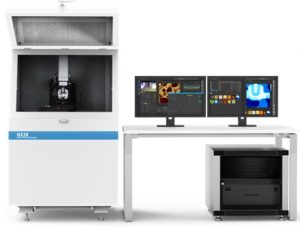
PARK SYSTEMS NX20 AFM
- Name: PARK SYSTEMS NX20 AFM
- Tool No.: MNCF 011
- Make : Park Systems
Atomic Force Microscope (AFM) is a very-high-resolution type of scanning probe microscope (SPM). It is designed to measure local properties, such as height, friction, magnetism, etc., with a sharp probe by raster scanning over a small area of a sample. Atomic force microscopy technique can demonstrate a vertical resolution of the order of fractions of a nanometer and also lateral resolution more than 20x times better than the optical diffraction limit
PARK SYSTEMS NX20 AFM
– Vertical resolution = 0.3nm, Lateral resolution = 2-10nm (depends on the tip), Scan range = 100x 100μm,
– Max vertical height/depth = 5μm
– KPFM (AM mode and Side-Band mode) , PFM, MFM, EFM, C-AFM, LFM, Nanolithography, Nano indentation, Force Spectroscopy
Technical Documents
- These will be updated soon.
Status: Operational
Sample Requirement: Flat and dry samples
Location: MNCF, Mechanical Bay
Training Videos:
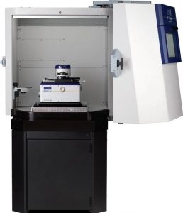
Additional NotesBRUKER DIMENSION ICON AFM -1
- Name: BRUKER DIMENSION ICON AFM -1
- Tool No.: MNCF 012
- Make : Bruker
Atomic Force Microscope (AFM) is a very-high-resolution type of scanning probe microscope (SPM). It is designed to measure local properties, such as height, friction, magnetism, etc., with a sharp probe by raster scanning over a small area of a sample. Atomic force microscopy technique can demonstrate a vertical resolution of the order of fractions of a nanometer and also lateral resolution more than 20x times better than the optical diffraction limit
BRUKER DIMENSION ICON AFM -1
– Vertical resolution = 0.3nm, Lateral resolution = 10nm (depends on tip) , Scan range = 90 x 90μm
– Max vertical height/depth = 5μm,
– PFM, KPFM(AM mode), MFM
– Nanolithography, EFM, LFM, Force Spectroscopy, PFQNM, ScanAsyst mode.
Technical Documents
- These will be updated soon.
Status: Operational
Sample Requirement: Flat, dry samples
Location: MNCF, Mechanical Bay
Training Videos:
Additional NotesBRUKER DIMENSION ICON AFM -2
- Name: BRUKER DIMENSION ICON AFM -2
- Tool No.: MNCF 013
- Make : Bruker
Atomic Force Microscope (AFM) is a very-high-resolution type of scanning probe microscope (SPM). It is designed to measure local properties, such as height, friction, magnetism, etc., with a sharp probe by raster scanning over a small area of a sample. Atomic force microscopy technique can demonstrate a vertical resolution of the order of fractions of a nanometer and also lateral resolution more than 20x times better than the optical diffraction limit
BRUKER DIMENSION ICON AFM -2
– Vertical resolution = 0.3nm, Lateral resolution = 10nm (depends on tip) , Scan range = 90 x 90μm
– Max vertical height/depth = 5μm,
– PFM, KPFM(AM mode) , MFM,
– Torsional mode AFM, EFM, LFM, Force Spectroscopy, PFQNM, ScanAsyst mode.
Technical Documents
- These will be updated soon.
Status: Operational
Sample Requirement: Flat, dry samples
Location: MNCF, Mechanical Bay
Training Videos:
Additional NotesAFM Dimension Icon Sys2
The Bruker Dimension Icon is a high-performance Atomic Force Microscope (AFM) designed for advanced nanoscale research. It offers high-resolution imaging, low drift, and noise levels, making it ideal for a wide range of applications. The system supports various imaging modes and techniques, including PeakForce Tapping for nanomechanical mapping.
General specifications :
- XY Scan Range: 90 μm x 90 μm
- Z Range: 7 μm
Microscope Optics:
- Digital Camera: 5 Megapixel
- Viewing Area: 180 μm–1465 μm
Operational in environment, up to 85 dBC continuous acoustic noise
Sample size up to 210 mm in diameter and ≤ 15 mm thick can be accommodated on the rotatable vacuum chuck.
The following imaging modes are available in AFM2: Bruker Dimension Icon:
Tapping mode: The cantilever oscillates near its resonance frequency, and the tip intermittently contacts the sample surface. In addition to topography, this mode can provide phase image of the sample. Phase image shows the phase lag between the oscillating probe and the drive signal. The phase lag is influenced by material properties like adhesion, viscoelasticity, and stiffness. Hence phase imaging can be used for distinguishing between different materials on the surface. It provides contrast based on material properties that are not visible in topography images alone.
Contact mode: The probe is in constant contact with the sample, providing high-resolution topographical images but can damage the soft samples. In force-distance spectroscopy of this mode, the tip approaches and retracts from the sample surface while measuring the vertical deflection of the cantilever. This generates force-distance curves that can be analysed to get information about the sample’s mechanical properties.
Scan Asyst mode: This mode is based on PeakForce Tapping, in which the AFM tip makes intermittent contact with the sample at a controlled frequency, applying a precise force to the sample surface. Unlike the Tapping Mode, which indirectly controls the force through oscillation amplitude, the applied peak force is directly controlled in this mode. In addition, the automatic adjustment of the imaging parameters like- setpoint, scan rate, and feedback gains in real time to optimize the imaging conditions makes it easier to use and provides consistent, high-quality topographical image.
Torsional Resonance Mode(TR Mode): To measure the lateral forces between the probe and the sample, which provides information about frictional properties and in-plane anisotropy. This mode is used for imaging topography, studying material properties, and characterizing 2D materials and heterostructures.
Peak Force Quantitative Nanomechanical Mapping (PFQNM): This mode is based on the Peak Force Tapping. It is used to map the mechanical properties like modulus, adhesion and dissipation while simultaneously imaging the topography of the sample. It is non-destructive and provides high-resolution data.
Lateral Force Microscopy (LFM): In this mode, the AFM tip is in constant contact with the sample surface. It measures the frictional force between the AFM tip and the sample by detecting the lateral deflection of the cantilever. Those mode is particularly useful for studying materials with anisotropic properties and for mapping variations in friction and adhesion across the sample.
Electrostatic Force Microscopy (EFM): This mode obtains the topography as well as the surface charge distribution of the sample by scanning tapping mode and lift mode. It first scans the sample surface in tapping mode to obtain topography and then the tip is lifted to predefined height above the sample surface. At the lifted height the scans the sample while applying the voltage to measure the electrostatic force between the tip and sample. Since the surface topography shapes the electric field gradient, significant differences in topography can obscure true variations in the field source. EFM is most effective with samples that have relatively smooth topography. Suitable field sources include trapped charges and applied voltages, and samples with insulating layers over conducting regions are also ideal for EFM.
Amplitude Modulated Kelvin Force Probe Microscopy (AM-KPFM): This mode measures the contact potential difference between the tip and the sample by nullifying the electrostatic force. It provides the topography as well as the quantitative results of local surface potential distribution from which the work function of the sample can be calculated.
Magnetic Force Microscopy (MFM): MFM using lift mode enables the imaging of weak, long-range magnetic interactions while minimizing topographical influence. The technique involves two scanning passes: the first acquires topographical data in TappingMode, and the second, at a predefined lift height, detects magnetic interactions. This method ensures that topographical features are virtually absent from the resulting MFM image, providing a clearer representation of magnetic properties.
Piezo Force response Microscopy (PFM): PFM is used to study the piezoelectric and ferroelectric domains. Vertical PFM images domains perpendicular to the surface, while horizontal PFM images domains parallel to the surface.
| Technique | Details Required |
| KPFM | Mode: AM KPFM/FM KPFM |
| C-AFM | Voltage to be applied on the sample (Mandatory for current mapping) |
| PFM | Mode (OFF resonance/Contact resonance/DART) Voltage for PFM spectroscopy (switching voltage) Voltage for Box-in-Box (if required) |
| Nano Indentation / PFQNM | Expected Young’s modulus value: (Mandatory for cantilever selection) |
| Nano Lithography | Specify type (Scratch lithography/Oxidation lithography)
Voltage for anodic oxidation lithography Expected scratch depth |
| MFM | Lift height: (If not specified, recommended lift height of 100 nm will be used; range: 30 nm to 150 nm) |
| Liquid Imaging | Mode (Contact/Tapping/Peak Force Tapping/PFQNM)
Liquid medium: (DI water assumed unless specified) |
Oxford MFP 3D Origin+
- Name: Oxford MFP 3D Origin+
- Tool No.: MNCF055
- Make : Oxford
The MFP-3D Origin+ is an extremely versatile and high performance research AFM ready for almost any field of research. It features the same core performance as the MFP-3D Origin but includes support for the complete range of innovative MFP-3D accessories.
Oxford MFP 3D Origin+
– Step Height (vertical resolution = 0.3nm, Lateral resolution = 10nm (depends on tip) , Scan range = 120x 120μm,
– Max vertical height/depth = 5μm
– PFM (DART, Vector, Vertical, Lateral PFM, High voltage PFM),
– KPFM(AM mode), MFM, EFM, C-AFM, LFM, Nanolithography, Force Spectroscopy,
– Humidty Setup
Technical Documents
- These will be updated soon.
Status: Operational
Sample Requirement: Flat, dry samples
Location: MNCF, Mechanical Bay
Training Videos:
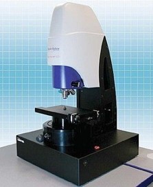
Additional NotesMicro System Analyzer (MSA 500)
Name: MICRO SYSTEM ANALYSER (MSA 500)
Tool No.: MNCF 014
Make : Polytec
- The Micro System Analyzer is the premier measurement tool for the analysis and visualization of structural vibrations and surface topography in micro structures such as MEMS. By fully integrating a microscope with scanning laser doppler vibrometry, stroboscopic video microscopy and scanning white light interferometry, the Micro System Analyzer is designed with an all-in-one combination of technologies that clarifies real microstructural response and topography.
- Polytec Micro System Analyzer combines three highly sophisticated measuring techniques in one instrument permitting a comprehensive investigation of a microstructure without moving the device to another test station..
Micro System Analyzer (MSA 500)
- Out of Plane vibrations:
– Frequency upto 20MHz
– Maximum displacement: ±75 nm
– Velocity resolution (rms): upto 1μm/s. - In-Plane Vibration:
– Frequency upto 1MHz
– Camera: 1.4 Megapixe
– Maximum velocity: 0.1 m/s … 10 m/s (magnification dependent) - Topography Analysis/Roughness/Thickness measurement (Even partially reflective samples)
Technical Documents
- These will be updated soon.
Status: Operational
Sample Requirement:
- MEMS/ PMUT Structures, Released structures, Gyroscopes, Piezoelectric materials
Location: MNCF, Mechanical Bay
Training Videos: 01 Micro System Analyzer.mp4
Additional NotesMicro UTM
- Name: Micro UTM
- Tool No.: MNCF 017
- Make : Mecmesin
A universal testing machine (UTM), also known as a universal tester, materials testing machine or materials test frame, is used to test the tensile strength and compressive strength of materials.
A universal testing machine (UTM), also known as a universal tester, materials testing machine or materials test frame, is used to test the tensile strength and compressive strength of materials. An earlier name for a tensile testing machine is a tensometer. The “universal” part of the name reflects that it can perform many standard tensile and compression tests on materials, components, and structures (in other words, that it is versatile).
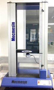
Micro UTM
– Available Load cell: 10N, 25N, 100N, 500N, 1 kN, 2.5 kN, 5 kN and 10 kN.
– Speed minimum 2 mm/min and maximum 1000 mm/min.
– Weight 140 kg (309 lb)
– MODES: Compression tester and tension testing.
– 400 mm (15.7″) clearance between columns.
Technical Document
- These will be updated soon.
Status: Operational
Sample Requirement: Samples must be prepared using ASTM standards
Location: MNCF, Mechanical Bay
Training Videos:
Additional NotesOptical Profilometer
- Name: Optical Profilometer (Taylor Hobson/Talysurf CCI)
- Tool No.: MNCF 016
- Make : Ametek
Profilometer is a measuring instrument used to measure surface profile, in order to quantify its roughness. Critical dimensions as step, curvature, flatness are computed from the surface topography. An optical profilometer is a non-contact method for providing much of the same information as a stylus based profilometer.
Optical profilometer uses Principle of Coherence Correlation Interferometry (CCI) in surface topography measurements. The CCI methods are based on the cross-coherence analysis of two low-coherent light beams, the object beam being reflected from the object , while the reference beam is reflected from a reference mirror.
– Vertical Resolution: 0.01nm
– Lateral Resolution: 0.4 to 0.6μM
– Maximum Measurement covering Area: 1.6mm*1.6mm
– X-Y Stitching: Advanced X, Y and Z stitching, extends the measurement range.(75mm)
– Pixels: 1024*1024
– Surface Reflectivity: 0.3% to 100%
Technical Documents
- These will be updated soon.
Status: Operational
Sample Requirement: Samples should be REFLECTIVE
Location: MNCF, Mechanical Bay
Training Videos:
Additional NotesRadiant System
- Name: Radiant System
- Tool No.: MNCF060
- Make : Radiant Technologies Inc
Meet the Precision Multiferroic II Ferroelectric Tester. It has a unique frequency rating of 270KHz at +/-100V built-in to the system. The Multiferroic II tester makes testing of thin films and bulk ceramics a fast and simple process. It captures 32,000 points at 2 MHz to achieve exquisite frequency resolution in DLTS or PAINT measurements.
The Precision Multiferroic II is offered with a variety of internal amplifiers. The Multiferroic II is offered with a ±100V, 200V and 500V built-in drive volt option. It can be expanded to 10kV with the addition of a high voltage interface and an amplifier.
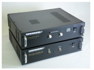
>Piezoelectric measurements like hysteresis,CV leakage tests,Fatigue analysis, PUND measurements.
High voltage measurements up to 10kV using TREK amplifier.
High temperature and low temperature measurements.
Technical Documents
- These will be updated soon.
Status: Operational
Sample Requirement:
Location: MNCF, Mechanical Bay
Training Videos:
Additional NotesRheometer
- Name: Rheometer
- Tool No.: MNCF 020
- Make : Anton Paar
A rheometer is a precision instrument that contains the material of interest in a geometric configuration, controls the environment around it, and applies and measures wide ranges of stress, strain, and strain rate. Rheometry refers to the experimental technique used to determine the rheological properties of materials; rheology being defined as the study of the flow and deformation of matter which describes the interrelation between force, deformation and time.
There are a number of rheometric tests that can be performed on a rheometer to determine flow properties and viscoelastic properties of a material, and it is often useful to deal with them separately
The cone and plate rheometer provides a measurement of shear stress and first normal stress difference in a geometry that results in a uniform shear rate throughout the shearing gap. The conical plate of 40mm and 50 mm, parallel plate 25 mm are available.
| Technical Data | MRC302 |
| Bearing | Air |
| EC motor | yes |
| Maximum torque | 200 nNm |
| Minimum torque rotation | 1 nNm |
| Minimum torque oscillation | 0.5nNm |
| angular deflection | 0.05 to ∞ µrad |
| Max. Speed | 314 rad/s |
| Min. angular frequency | 10-7 rad/s |
| Max. angular frequency | 628 rad/s |
| Normal force range | 0.005-50 N |
| Normal force resolution | 0.5 mN |
| Temperature range | 20 to 100 ℃ |
| Operations : Amplitude sweep , frequency sweep, temparture dependent and other operations performed in a standard mode. |
Technical Documents
- These will be updated soon.
Status: Operational
Sample Requirement: Liquid and non-corrosive samples
Location: MNCF, Mechanical Bay
Training Videos: https://indianinstituteofscience.sharepoint.com/:v:/s/rheometerusersgroup/EW7qsoeV8VZGmwQnffQUWbsBzuuxJ1Z_VCFyu_YQR2N-tw?e=Dcfgp1
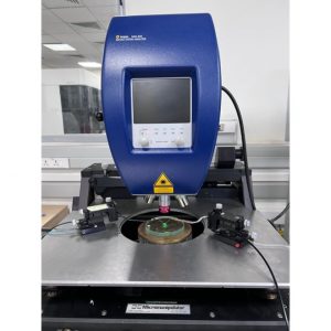
Additional NotesScanning Acoustic Microscope
- Name: Scanning Acoustic Microscope
- Tool No.: MNCF 015
- Make : KSI
A scanning acoustic microscope (SAM) is a device which uses focused sound to investigate, measure, or image an object (a process called scanning acoustic tomography). It is commonly used in failure analysis and non-destructive evaluation. It also has applications in biological and medical research. The semiconductor industry has found the SAM useful in detecting voids, cracks, and delaminations within microelectronic packages.
Scanning acoustic microscopy works by directing focused sound from a transducer at a small point on a target object. Sound hitting the object is either scattered, absorbed, reflected (scattered at 180°) or transmitted (scattered at 0°). It is possible to detect the scattered pulses travelling in a particular direction.
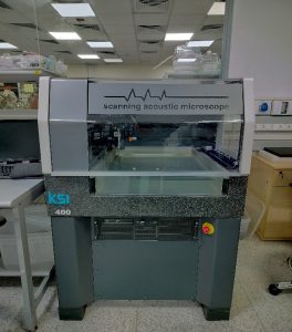
Scanning Acoustic Microscope
– Measurements like Delamination, Finding out the voids, Bonding and internal structures or breakages.
– Transducers: 50,100, 150. 230 MHz
– Scanning range from 200µmx200µm to 400 mmx400mm
– 625x magnification
– Outstanding high scanning speed: 2000 mm/s
Technical Documents
- These will be updated soon.
Status: Operational
Sample Requirement: MEMS/ PMUT Structures, Released structures, Gyroscopes, Piezoelectric materials
Location: MNCF, Mechanical Bay
Training Videos:
Additional Notes