SEM with EDS
- Name: Ultra55 FE-SEM Carl Zeiss EDS
- Tool No: MNCF 021
- Make : Carl Zeiss India Pvt. Ltd
- The ultra high resolution Field emission scanning electron microscope coupled with material spectroscopy tools. The ULTRA 55 represents the latest development in GEMINI technology, a fully integrated High-definition angular selective Backscattered electron (HDAsB) detector. The ULTRA 55 offers ultra high resolution for both SE to image surface information and BSE to present compositional information. The new HDAsB detector features an integrated filtering grid to enhance image quality and requires no additional adjustments. The HDAsB detector is less sensitive for edge contrast and charging effects which enables precise imaging and measurement of boundaries, particles, and features. Combined with the large multi-port analytical chamber, the fully motorised 5-axes motorised eucentric stage and the GEMINI high current mode.
- The SEM tool is also equipped with Oxford EDS, energy dispersive spectroscopic (EDS) detector and INCA software for compositional analysis and elemental mapping.
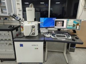
Zeiss ULTRA 55 Field Emission-Scanning Electron Microscope.
– Resolution: 0.8 nm at 15 kV; 1.6 nm at 1kV :
– Accelerating Voltage: 0.02 – 30 kV in steps of 10 V (for imaging, accelerating voltage upwards of 200 V is suggested) (8 KeV column Potential : Beam Booster)
– Probe current in the range 4 pA to 20 nA
– Six beam defining multi hole apertures (7.5µm, 10µm, 20µm, 30µm, 60µm and 120µm).
– Specimen chamber: 330 mm (inner diameter), 270 mm height
– Specimen stage: 5-axes motorized eucentric (eucentric position is the horizontal center of the objective lens), controlled via a Zeiss software
– Specimen stage movement: X/Y = 130 mm, Z=50 mm, T= -4⁰ to 70⁰, R= 360⁰ continuous
– Permissible specimen weight: up to 0.5 kg
– Detectors: In-lens, SE2 (ET), BSE – HDAsB (only in SEM-EDS system, Oxford EDAX with Inca 5.05 EDS system.
– Patented electromagnetic/electrostatic Gemini objective lens assembly
– Eight pole stigmator
Technical Documents
- These will be updated soon.
Status: Operational
Sample requirement:
- Sample should not have any moisture / sample should not de-gas in high vaccum
Location: MNCF, Materials Bay
Training Videos: SEM training vedio_12 Oct 2020_Draft 1.mp4
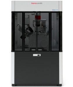
Additional NotesFIB-HELIOS 5 UX DUAL BEAM
- Name: FIB-Helios 5 UX Dual Beam
- Tool No.: MNCF 053
- Make : Thermofisher Scientific
Thermo Scientific’s Helios 5 UX combining the innovative Elstar™ electron column with high-current UC+ technology to generate better material contrast and higher resolution imaging. The Phoenix™ Focused Ion Beam (FIB) Column by Thermo Scientific is an advanced tool that permits the fastest, simplest and most precise preparation of high-quality samples. In addition, the Helios 5 UX DualBeam has a range of modern techniques for simple, repeatable S/TEM sample preparation together with its advanced electron and ion optics. It also provides top subsurface characterization, patterning and 3D analysis, even in more difficult samples.
1.Electron optics
- Elstar extreme high-resolution field emission SEM column with: Magnetic immersion objective lens, High-stability Schottky field emission gun to provide stable high-resolution analytical currents, UC+ monochromator technology.
2.Electron beam resolution
- At optimum WD: 0.6 nm at 30 kV STEM; 0.7 nm at 1kV; 1.0 nm at 500 V (ICD)
- At coincident point: 0.6 nm at 15kV; 1.2 nm at 1kV
3.Electron beam parameter:
- Electron beam current range: 0.8 pA to 100 nA; Accelerating voltage range: 350 V – 30 kV; Maximum horizontal field width: 2.3 mm at 4 mm WD
4. Ion optics
- Phoenix Ion Column with superior high-current and low-voltage performance
- Ion beam current range: 1 pA – 65 nA
- Accelerating voltage range: 500 V – 30 kV
- Ion beam resolution at coincident point: 4.0 nm at 30 kV using preferred statistical method
5. Detectors
- Elstar in-lens SE/BSE detector (TLD-SE, TLD-BSE)
- Elstar in-column SE/BSE detector (ICD)
- Elstar in-column BSE detector (MD)
- Everhart-Thornley SE detector (ETD)
- IR camera for viewing sample/column
- High-performance in-chamber electron and ion detector (ICE) for secondary ions (SI) and electrons (SE)
- Retractable STEM 3+ detector with BF/ DF/ HAADF segments
Technical Documents
- These will be updated soon.
Status: Operational
Sample requirement: Follow the sample preparation document
Location: Material Bay, MNCF
Training Videos: Overview of Dual Column Focused Ion Beam.mp4
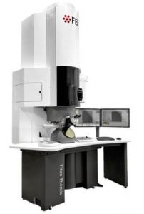
Additional NotesTEM-TITAN Themis D3391
- Name: TEM- Titan 300 Themis D 3391
- Tool No.: MNCF 027
- Make : Thermo Fisher Scientific
The Titan 300 Themis D 3391 model is equipped with field emission gun ( Schottky ) at 300 kV operating voltage. It is capable of doing morphology, structure and chemical analysis using parallel (TEM) and convergent (STEM) beams at atomic resolution. In addition to this we can do the magnetic structure studies using the Lorentz microscope.
We also have the capability for In-situ studies with heating and biasing.
- X-FEG Schottky emission gun (Energy Spread 0.7 eV) operative up to 300kV with the column having triple condenser lens system.
- Piezo enhanced with 5-axis specimen compu-stage.
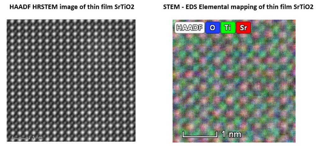
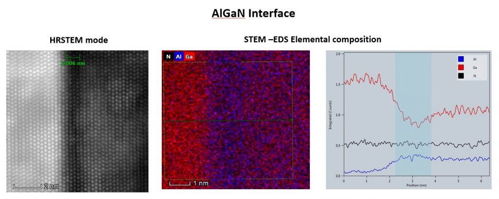
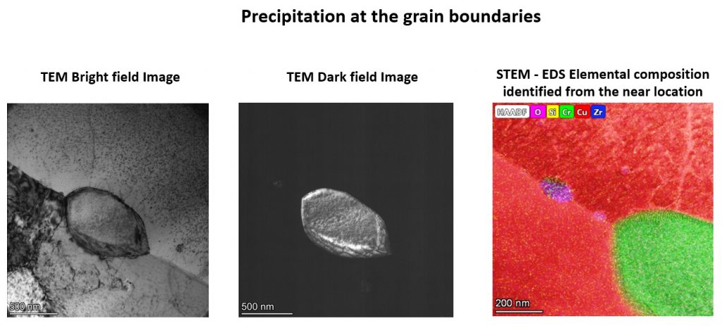
- 4K x 4K CMOS camera for data acquisition and with a Super-X EDS four quadrant detectors for ultra-fast EDS data collection through point/line scans and hypermaps.
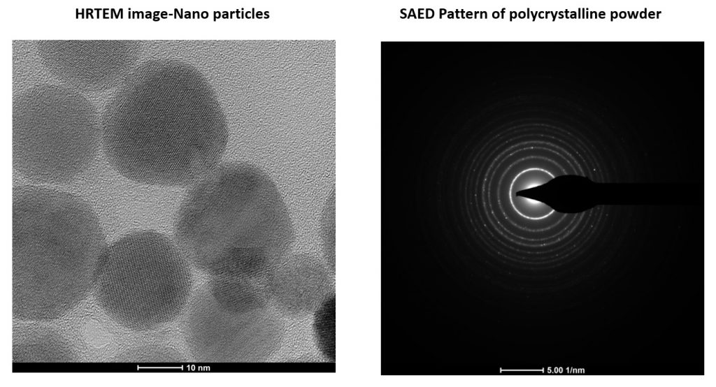
- Resolution: High-Resolution parallel beam (HRTEM): 0.19 nm
High-Resolution Scanning-TEM (STEM): 0.136 nm
Lorentz: 1.5 nm - Magnification for imaging: 1. LM 45 x to 1.2 Mx for TEM.
2. 5000 x to 165 Mx for STEM.
| Conventional TEM | STEM | Lorenz (In TEM mode) | DPC ( In STEM mode) | CBED ( In TEM/STEM mode) |
| -Imaging
-High resolution (HRTEM) -Selected area electron diffraction |
-HAADF Imaging
-EDS spectra (spot, line and area) -EDS mapping |
– Magnetic imaging | – Visualizing the electromagnetic field in the specimen | -Space group of the crystal
– Precise lattice parameter from smaller area. |


Technical Documents
- These will be updated soon.
Status: Operational
Sample requirement: non-magnetic samples such as metals, semiconductors, powders and solution-based nanoparticles (completely dried and desiccated). Samples have to be high vacuum compatible.
Location: MNCF, TEM room
Training Videos:
Additional NotesX-Ray Photoelectron Spectroscopy
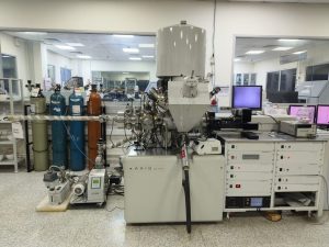
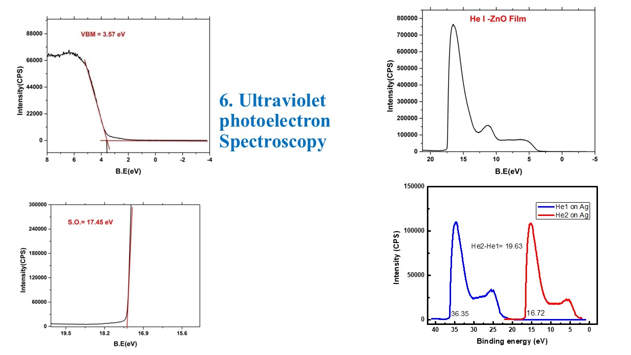
- Name: X-Ray Photoelectron Spectroscopy
- Tool No.: MNCF 026
- Make : Kratos Analytical, UK
-XPS tool for materials identification and analysis, and advanced studies AXIS ULTRA DLD, integrates the Kratos patented Magnetic Immersion Lens and Charge Neutralisation System coupled with Spherical Mirror Analyser.
-The Spherical Mirror Analyser provides real time chemical state and elemental imaging using the full range of pass energies and multi-point analysis from either real time or scanned images without the need for sample translation.
-A microchannel plate and phosphor detection system are incorporated into the system to provide a parallel imaging capability with high spatial resolution and high sensitivity. Advanced zoom optics enable a variable viewing area for the identification of macro or micro features.
X-Ray Photoelectron Spectroscopy
1. The AXIS Ultra DLD uses a 500 mm diameter Rowland circle monochromator of Quartz crystal.
2. 165mm mean radius hemispherical analyzer for spectroscopy.
3. Tool resolution XPS: 0.44 eV for Ag 3d 5/2 resolution proof. (Prsesnt 0.6eV)
4. Tool resolution UPS resolution (Difference between He 1- He2 19.5 eV (Present 19.6eV)
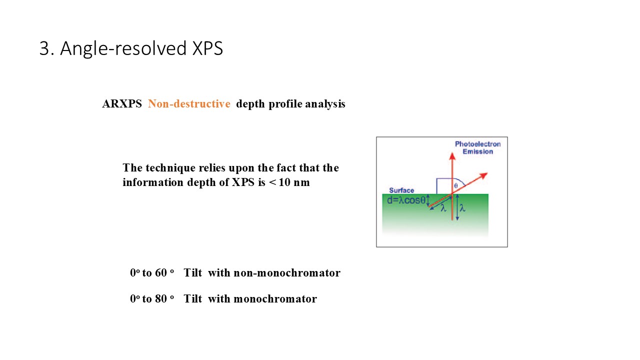
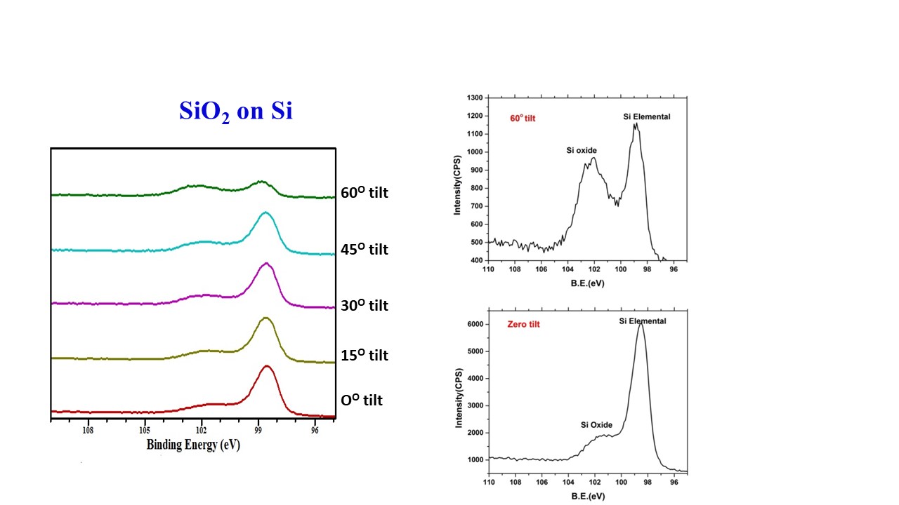
5. Surface sensitivity – photoelectron signal from first 1-10 layers of atoms and molecules.
6. Identification of all elements (except H & He) at concentrations >0.1atomic
7. Elements detected: From Lithium to heavy metals
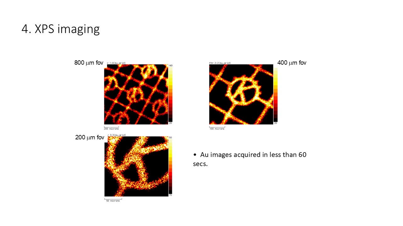
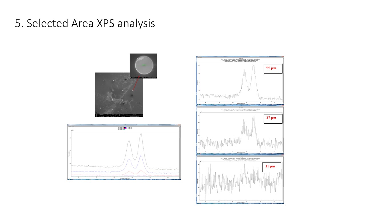
8. Lateral variations in surface composition at 15µm resolution.
9. Depth resolution: 2 to 8 nm
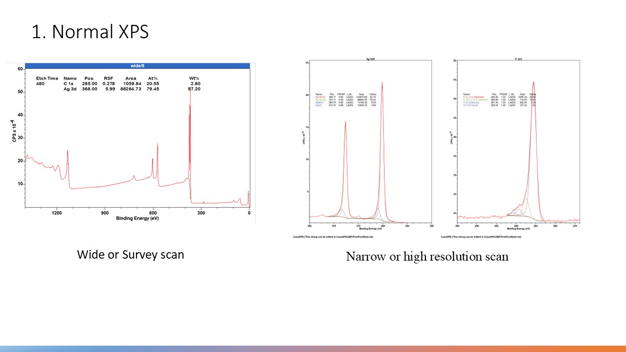
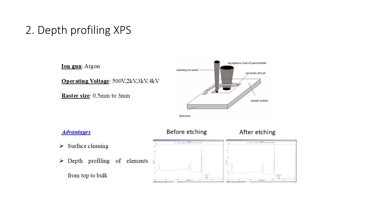
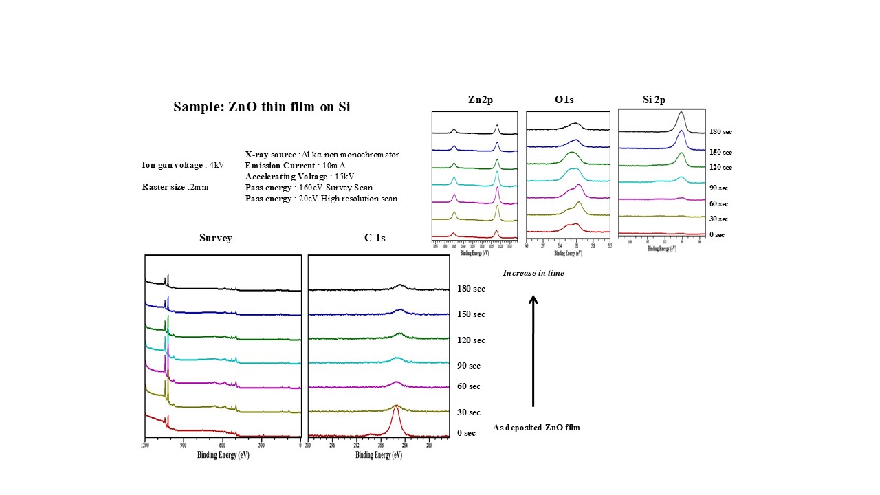
Modes:
- Normal XPS
- Depth profiling XPS
- Angle-resolved XPS
- XPS imaging
- Selected area XPS
- Ultra-violet photoelectron spectroscopy (UPS)
Technical Documents
- These will be updated soon.
Status: Operational
Sample requirement: Sample dimension must be 5±2 mm and height no more than 5 mm. Anything more in size than specification (5±2 mm), especially thin film will be treated as additional samples and more slots will be required accordingly. Please mark the top side of sample in case of thin films.
S, Pb, I, Sn, Zn, Ga, In based materials are strictly not allowed for etching,only elemental XPS (survey or high-resolution scans) allowed for those samples
Location: MNCF, Materials Bay
Training Videos: XPS Video
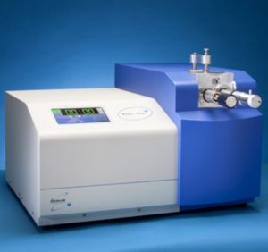
Additional NotesUltra55 FE-SEM Carl Zeiss mono
- Name: Ultra55 FE-SEM Carl Zeiss mono
- Tool No: MNCF 022
- Make : Gatan UK
- The cathodolumiescence (CL) detector attached to a SEM is capable of producing high resolution CL images of luminescent materials.
- CL emissions have been used in numerous petrologic studies of minerals (like quartz, zircon, diamond, carbonates, etc.) from a variety of geologic environments. For example, it is used in identifying trace elements contained in minerals or production of mechanically induced defects in the crystals because CL can illuminate textures which are not observable by other methods (like transmitted light, SE, BSE, etc.). Therefore, CL can provide important information on the optical and electronic properties of a material.
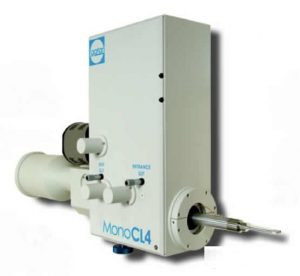
Ultra55 FE-SEM Carl Zeiss mono.
· Focal length: 300 mm
· Aperture: f/4.2
· Gratings: Plane gratings. Choice of two with software recognition
· Grating Size: 69 x 69 mm
· Wavelength range ~0.6 to 1.5 times the blaze wavelength
· Slits: Continuously variable from 10 mm to 5 mm
· Dispersion: 2.7 nm/mm for 1200 l/mm grating
· Resolution: grating dependent, maximum ~0.5nm
· Wavelength accuracy: ± 0.2nm, automated backlash removal. Position determined by software.
Technical Documents
- These will be updated soon.
Status: Operational
Sample requirement: Thin films, powders, metals, polymers, biological samples
Location: MNCF, Materials Bay
Training Videos: MonoCL_Spectrum and Imaging.mp4
Additional NotesDimpler
- Name: Dimpler
- Tool No.: MNCF 046
- Make : GATAN
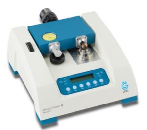
The Dimple Grinder II provides rapid material removal with minimal damage and offers a fast and reliable mechanical method of pre-thinning to near electron transparency.
The dimple grinder is equipped with a dual measuring system – a digital, electronic micrometer with a readout accuracy of 1 μm.
Maximum allowance of the dimensions of the specimen : 100 μm thick * 3 mm diameter
Status: Operational
Sample requirement:
- Maximum allowance of the dimensions of the specimen : 100 μm thick * 3 mm diameter
- Ceramics, semiconductors, metals, and combinations thereof
Location: Materials Bay
Additional NotesUltrasonic Disc cutter(Model 651)
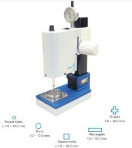
- Name: Ultrasonic Disc cutter(Model 651)
- Tool No.: MNCF 045
- Make : GATAN
Used for Cutting simple holes, unique shapes or transmission electron microscope (TEM) discs from hard or brittle materials such as semiconductors , ceramics and geological materials ranging from <1 – 10 mm in size and from <0.04 – 5 mm in thickness.
Status: Operational
Sample requirement: Can cut simple holes, unique shapes, or TEM discs from hard, brittle materials such as semiconductors, ceramics, and geological samples, in thicknesses ranging from < 40 µm to 5 mm
Location: Materials Bay
Additional NotesPlasma Cleaner
- Name: Plasma Cleaner
- Tool No.: MNCF 043
- Make : Model 1070 Nano Clean-Fischione Instruments
- Function: Cleans specimens and holders immediately before insertion into an electron microscope.
- Benefits: Removes carbonaceous debris, preventing contamination during imaging and analysis.
- Capacity: Accommodates two electron microscopy specimen holders.
- Features: Includes multiple gas inlets with mixing capabilities.
Status: Operational
Sample requirement: Compatible with TEM specimen holders for transmission electron microscopes. Ion energies less than 12 eV as a function of the downstream plasma
Location: Materials Bay
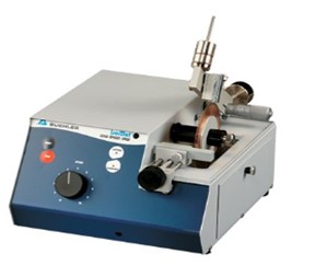
Additional NotesLow Speed SAW – Isomet
- Name: Low Speed SAW – Isomet
- Tool No.: MNCF 042
- Make : BUEHLER
It is a precision sectioning saw designed for cutting various types of Materials with minimal deformation and high quality of cut used for TEM sample preparation and sample sectioning analysis.
Maximum Sample dimension allowance : 5 cm * 5 cm * 5cm
Status: Operational
Sample requirement:
- IsoMet Low Speed Saw has the capability to cut virtually any material including brittle or ductile metals, composites, cements, laminates, plastics, electronic devices, and biomaterials.
- Maximum Sample dimension allowance : 5 cm * 5 cm * 5cm
Location: Materials Bay
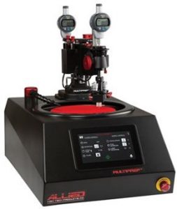
Additional NotesMultiPrep 8″ Precision Polishing Systems
- Name: MultiPrep 8″ Precision Polishing Systems
- Tool No.: MNCF 041
- Make : Allied
The MultiPrep™ System is a programmable machine that enables precise semiautomatic sample preparation of a wide range of materials for microscopic (optical, SEM, FIB, TEM, AFM, etc.) evaluation.
Applications :SIMS Thinning , serial sectioning, TEM Wedge Thinning , Thin Sectioning , EBSD preparation , Circuit Delayering, Precision Cross-sectioning, Optics/Optical device Polishing
Status: Operational
Sample requirement: Brittle materials like ceramics, geological materials and semiconductors
Location: Materials Bay
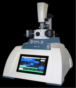
Additional NotesPIPS II Model 695
- Name: PIPS II Model 695
- Tool No.: MNCF 040
- Make : GATAN
Precision Ion polishing system is an Ion milling process used for precise thinning at the region of interest by precise centering , control of the Ion beam (Argon).
The specimens can be cooled to Liquid Nitrogen Temperatures.
Status: Operational
Sample requirement:
- 3mm dia with thickness less than 40 µm
- Brittle materials like ceramics, geological materials and semiconductors
- Ductile materials like metals and alloys
Location: Materials Bay
Additional NotesGold Sputtering- Quorum
- Name: Gold Sputtering- Quorum
- Tool No.: MNCF 023
- Make : Quroum Technologies
– The Q150R system is a versatile sputter coater/carbon evaporator for preparing specimens for examination by electron microcopy. The instrument is fully adaptable to a wide range of specimens and offers easy loading and unloading of samples. The changeover between sputtering and evaporation inserts is simple. The system is fully automated with a user defined profile controlling the pumping sequence, preheating, outgassing, the time and number of evaporation/sputter bursts, and the current used during the process. The Q150R features a rotary vacuum pumped chamber controlled by the instrument throughout the fully automatic coating cycle
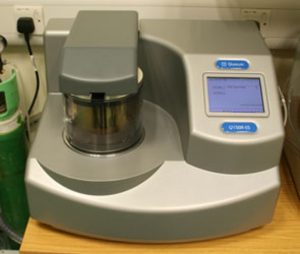
Gold Sputtering- Quorum
– Sputter Current – 80 (mA)
– Tooling Factor – 10
– Sputter Time – 3600 (seconds)
– Terminate Thickness – 2000 (nm)
– Maximum Sputter Time – 60 (minutes)
Technical Documents
- These will be updated soon.
Operating manual: 242277287-Q150R-5-pdf.pdf
Status: Operational
Sample requirement: NA
Location: MNCF, Materials Bay
Training Videos:
Additional NotesGold Sputtering-Jeol
- Name: Gold Sputtering-Jeol
- Tool No.: MNCF 024
- Make : Jeol
– Thin film conductive coatings are effective in eliminating charging with non-conductive materials or enhancing secondary electron emission. JEOL’s Smart Coater is a fully automated sputter coater that applies a fine-grained gold or platinum (option) coating on samples for imaging in.
– This coater uses a low voltage discharge technique with a magnetron electrode for high efficiency, cold sputtering. Low voltage sputtering, as well as having the sample isolated from the electrode, minimizes sample damage.
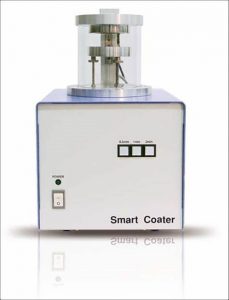
Gold Sputtering-Jeol
– Pressure – ~4 Pa
– Chamber Size 86mm (d) x 100mm (h); hard glass
– Temperature 15~30 °C (59~86 °F)
– Humidity Less than 70%
– Power Single Phase AC 100V/115V, 50/60 Hz, 650VA
– Ground Grounding Terminal (one, 100Ω or less)
– Sputter Unit
– Size/Weight
– 203mm (w) x 270mm (d) x 325mm (h); 6 kg
– RP 120mm (w) x 289mm (d) x 163mm (h); 9.3 k
Technical Documents
- These will be updated soon.
Operating manual: Technical note-Sample Preparation – Coating.pdf
Status: Operational
Sample requirement: NA
Location: MNCF, Materials Bay
Training Videos:
Additional NotesCritical Point Dryer
- Name: Critical Point Dryer
- Tool No.: MNCF 051
- Make : Quroum Technologies
The K850 Critical Point Dryer (see Figure 1-1) is designed for use with CO2 having first replaced any water in the specimen by a series of dehydration, often in the same fluid such as acetone or ethanol, which will also be the intermediate fluid.
Critical point drying is so named as it includes, as part of its process, the occurrence known as the continuity of state for which there is no apparent difference between the liquid and gas state of a medium, the surface tension between this interface reducing to zero. This occurs at a specific temperature and pressure with resulting density and is known as the critical point. This condition of zero surface tension can be used to dry biological specimens, avoiding the damaging effects of surface tension.
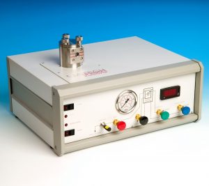
Critical Point Dryer
– Operating Temperature Normal operating temperature 35 °C (critical temperature 32 °C
– Operating Pressure 1350 psi (critical pressure 1172 psi)
– Pressure Safety Cut-out 1700 psi
– Safety Pressure Bursting Disc 1765-2040 psi
– Site Considerations Requires space for CO2 cylinder
– Electrical 230V 50Hz (3 A max) 115V 60Hz (6 A max
Technical Documents
- These will be updated soon.
Status: Operational
Sample requirement: Used to dry biological specimens, avoiding the damaging effects of surface tension
Location: MNCF, TEM room
Training Videos: CPD video.mp4
Additional Notes