
UHR Dual Beam FIB System: Helios NanoLAB 600i (FEI)
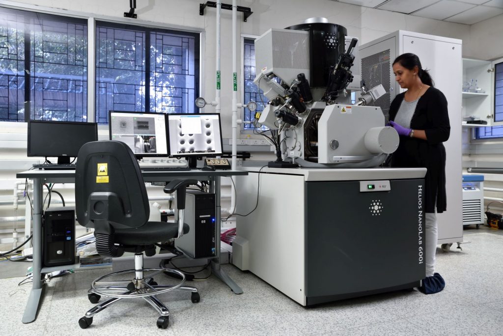
Powerful electron and ion beam tool for imaging, patterning and precise TEM sample preparation Advanced DualBeam for ultra-high resolution imaging, analysis and fabrication at the nanoscale. This FEI tool offers advances in the ion beam, electron beam, patterning and a range of features to make milling, imaging, analysis and sample preparation down to a nanoscale, standard applications in the lab.
General Features:-
- Electronics3D Metrology
- Defect & Failure Analysis.
- TEM Lamella Preparation
- Materials Science Prototyping for MEMS and NEMS
- Nanometrology of Critical Dimensions at the Nanoscale
- High Quality Sample Preparation Using Focused Ion Beams
- Natural ResourcesCuttings, Drill Cores, and Plugs Electron beam resolution @ optimum WD (0.8nm at 30kV (STEM), 0.9 nm at 15 kV, 1.4 nm at 1 kV)
- Electron beam resolution @ coincident point (1.0 nm at 15 kV, 1.6 nm at 5 kV, 2.5 nm at 1 kV)
- Ion beam resolution @ coincident point (4.5 nm at 30 kV using preferred statistical method (2.5 nm at 30kV using selective edge method Maximum horizontal field width
SEM with EDS
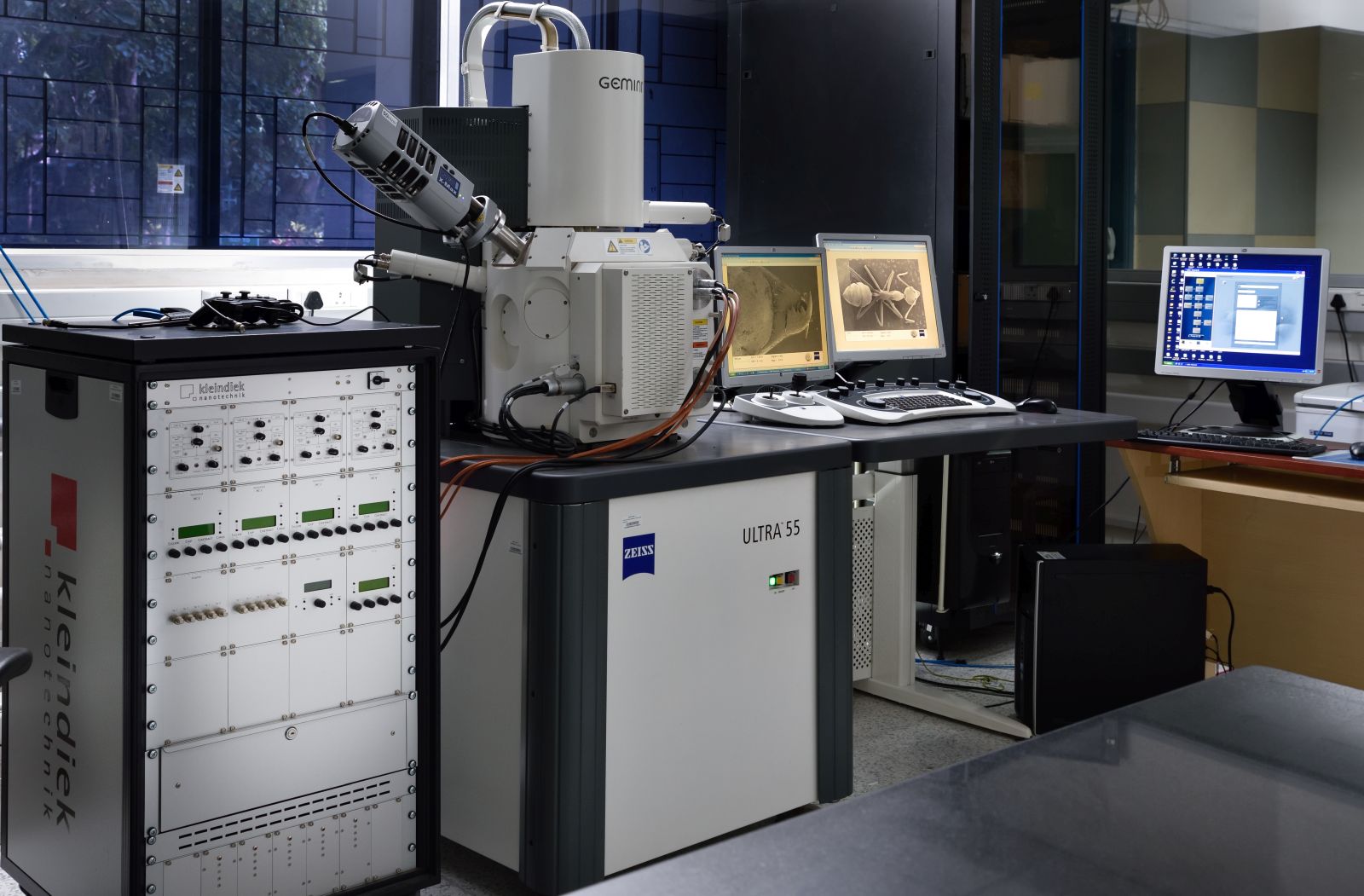
Ultra high resolution scanning electron imaging coupled with material spectroscopy tools The ULTRA 55 represents the latest development in GEMINI technology. Based on the SUPRA 55, the ULTRA 55 now comprises a fully integrated Energy and angle selective Backscattered electron (EsB) detector. The ULTRA 55 offers ultra high resolution for both SE to image surface information and BSE to present compositional information. The new EsB detector features an integrated filtering grid to enhance image quality and requires no additional adjustments. The EsB detector is less sensitive for edge contrast and charging effects which enables precise imaging and measurement of boundaries, particles, and features. Combined with the large multi-port analytical chamber, the fully motorised 5-axes motorised eucentric stage and the GEMINI high current mode the ULTRA 55 also offers superb analytical capabilities.
General Features:-
- Ultra high resolution imaging at low kV
- Fully integrated EsB detector for compositional information
- Low kV BSE imaging at short working distance: WD = 1mm
- High efficiency In-lens SE detector for high contrast surface imaging
- GEMINI technology with high efficiency In-lens detector for high contrast topographic imaging
- Easy operation through Windows XP based SmartSEM control software
- Local Charge Compensator in ULTRA PLUS for imaging of non-conductive specimen
SEM with MonoCL
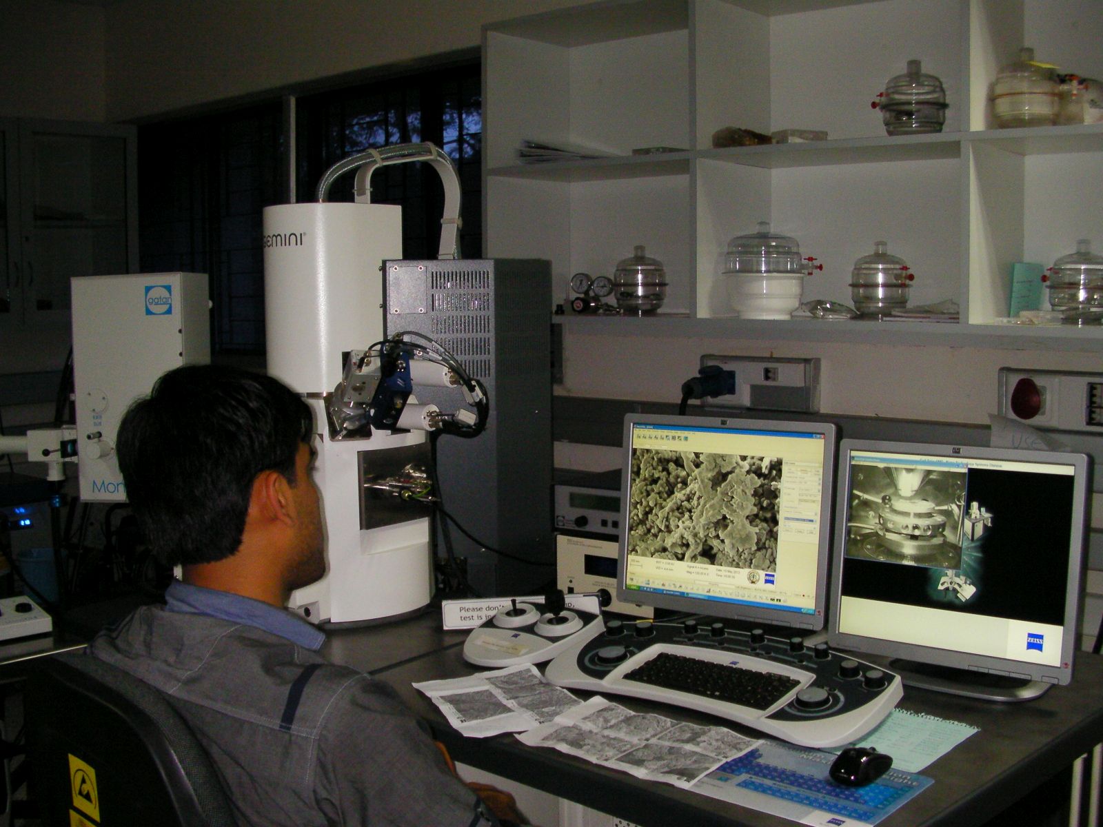
Ultra high resolution scanning electron with monochromatic imaging spectroscopy tools
General Features:-
- Panchromatic and monochromatic imaging with high spatial and spectral resolution
- Point and click selection of spectroscopy, imaging and mapping modes
- Shortpass, longpass and bandpass imaging using filter options for increased flexibility
Multi-technique X-ray Photoelectron Spectroscopy with XPS-mapping capability
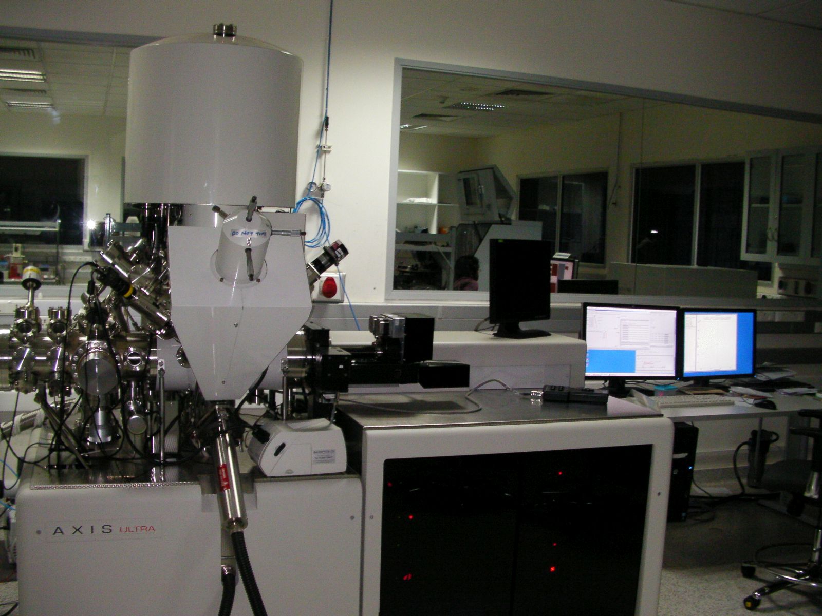
XPS tool for materials identification and analysis, and advanced studies AXIS ULTRA, a natural evolution from the AXIS 165, integrates the Kratos patented Magnetic Immersion Lens and Charge Neutralisation System with our new, patented Spherical Mirror Analyser. The Spherical Mirror Analyser provides real time chemical state and elemental imaging using the full range of pass energies and multi-point analysis from either real time or scanned images without the need for sample translation. A microchannel plate and phosphor detection system are incorporated into the system to provide a parallel imaging capability with high spatial resolution and high sensitivity. Advanced zoom optics enable a variable viewing area for the identification of macro or micro features. The instrument’s exceptional small spot capabilities (< 15 microns) are achieved via a combination of the magnetic lens and selected area apertures. The AXIS line of multi-technique photoelectron spectrometers provides scientists with unsurpassed performance for applications which require high energy resolution and high spatial resolution, high sensitivity, time efficiency and ease of use.
General Features:-
- High Energy Resolution and Charge Neutralisation.
- Fast Parallel Imaging
- Multi-point Spectroscopy
- Exceptional small spot capabilities (15 micron)
- Charge neutralization feature for insulating samples.
- Quantitative chemical imaging of surfaces
Transmission Electron Microscope (Titan Themis 300kV from FEI, now Thermo)
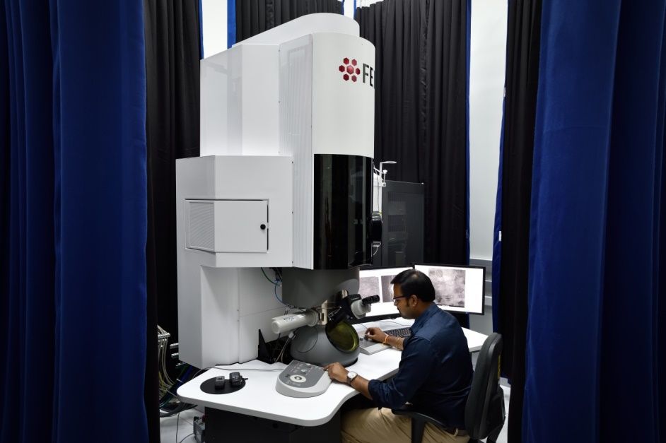
Measurement capabilities include the following:-
- Ultra-bright XFEG gun
- 60-300kV, suitable for beam-sensitive samples
- 4K x 4K CMOS camera
- Single tilt and double tilt specimen holders
- New computerized 5-axis specimen piezo-stage
- Super-X quad EDS detector for super-fast elemental analysis
- EDX Solid State Detector
- HRTEM and STEM mode
- HAADF (High Angle Annular Dark Field Imaging) and triple Dark Field/Bright Field (DF/BF) detectors for simultaneous imaging in STEM mode
- SAED (Selected Area Electron Diffraction)
Sample Preparation Techniques
JEOL Smart Coater
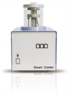
Specifications:
Gold (Au) Target:
Coating condition : Sample at 20mm (WD)
Resulting thickness:5nm at 1min, 10nm at 2min
General Use: Applies a thin film conductive coating to the sample that is effective in eliminating charging of non-conductive materials or enhancing secondary electron emission.
K850 Critical Point Dryer
General Use: It is an efficient technique for drying the delicate samples for SEM and TEM and used in Biological, MEMS and many other research areas.
Maximum Sample dimension allowance : 0.8 mm * 0.8 mm * 1 mm (thickness)
BUEHLER Iso Met LOW SPEED SAW
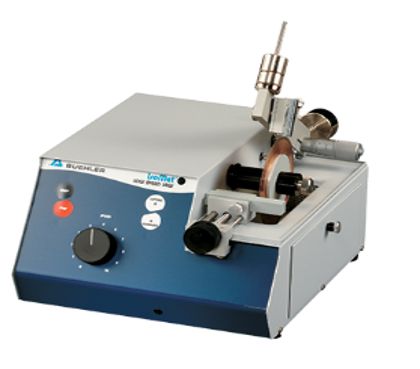
General Use: It is a precision sectioning saw designed for cutting various types of Materials with minimal deformation and high quality of cut used for TEM sample preparation and sample sectioning analysis.
Maximum Sample dimension allowance : 5 cm * 5 cm * 5cm
Allied High Tech MultiPrep 8″ PRECISION POLISHING SYSTEMS
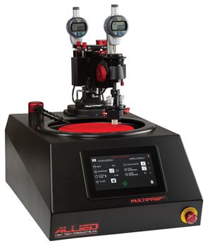
The MultiPrep™ System is a programmable machine that enables precise semiautomatic sample preparation of a wide range of materials for microscopic (optical, SEM, FIB, TEM, AFM, etc.) evaluation.
Applications :SIMS Thinning , serial sectioning, TEM Wedge Thinning , Thin Sectioning , EBSD preparation , Circuit Delayering, Precision Cross-sectioning, Optics/Optical device Polishing
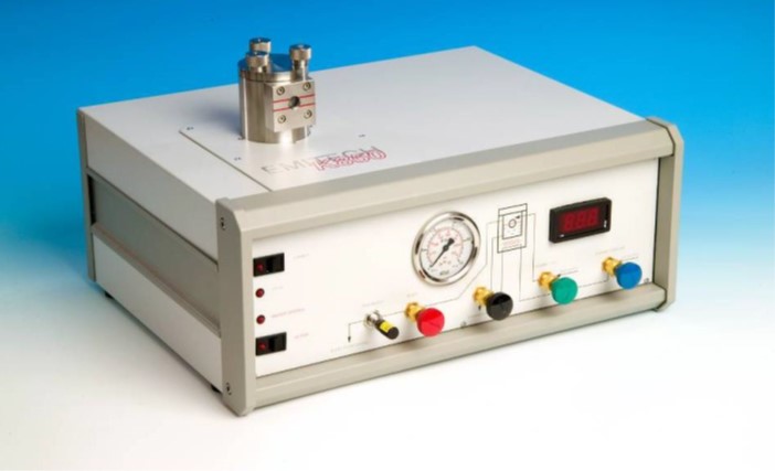
GATAN PIPS II Model 695
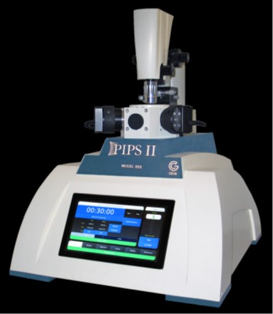
General Use: Precision Ion polishing system is an Ion milling process used for precise thinning at the region of interest by precise centering , control of the Ion beam (Argon).
The specimens can be cooled to Liquid Nitrogen Temperatures.
Fischione Model 1070 Nano Clean
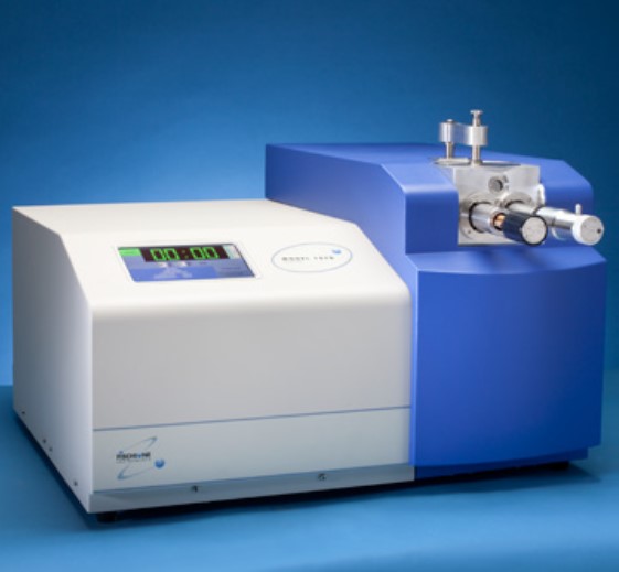
General Use: Cleans specimens and holders immediately before insertion into an electron microscope; removes existing carbonaceous debris from the specimen and prevents contamination during imaging and analysis.
GATAN Dimple Grinder II (Model 657)
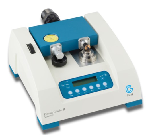
General Use : The Dimple Grinder II provides rapid material removal with minimal damage and offers a fast and reliable mechanical method of pre-thinning to near electron transparency.
The dimple grinder is equipped with a dual measuring system – a digital, electronic micrometer with a readout accuracy of 1 μm.
Maximum allowance of the dimensions of the specimen : 100 μm thick * 3 mm diameter
GATAN Ultrasonic cutter(Model 651)
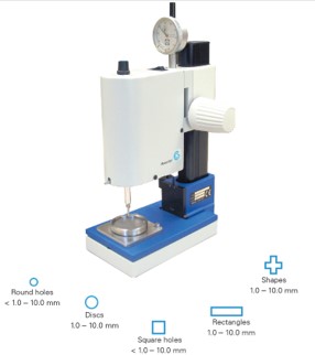
General Use: Used for Cutting simple holes, unique shapes or transmission electron microscope (TEM) discs from hard or brittle materials such as semiconductors , ceramics and geological materials ranging from <1 – 10 mm in size and from <0.04 – 5 mm in thickness.
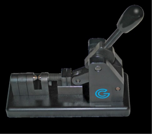
GATAN Disc Punch
General Use: Used for rapidly cutting transmission electron microscope (TEM) discs from ductile and soft materials and used for preparing specimen discs of 3 mm in diameter and material thicknesses ranging from 10 μm to above 100 μm for transmission electron microscopy.